Tuesday, September 16, 2008

Verilog Questions

Q: What is the difference between a Verilog task and a Verilog function?

A:

The following rules distinguish tasks from functions:

1. A function shall execute in one simulation time unit

A task can contain time-controlling statements.


2. A function cannot enable a task

A task can enable other tasks or functions.


3. A function shall have at least one input type argument and shall not have an output or inout type argument;

A task can have zero or more arguments of any type.


4. A function shall return a single value;

A task shall not return a value.


Q: Given the following Verilog code, what value of "a" is displayed?

always @(clk) begin

a = 0;

a <= 1;

$display(a);

end

A:


This is a tricky one! Verilog scheduling semantics basically imply a four-level deep queue for the current simulation time:

1: Active Events (blocking statements)

2: Inactive Events (#0 delays, etc)

3: Non-Blocking Assign Updates (non-blocking statements)

4: Monitor Events ($display, $monitor, etc).

Since the "a = 0" is an active event, it is scheduled into the 1st "queue". The "a <= 1" is a non-blocking event, so it's placed into the 3rd queue. Finally, the display statement is placed into the 4th queue. Only events in the active queue are completed this sim cycle, so the "a = 0" happens, and then the display shows a = 0. If we were to look at the value of a in the next sim cycle, it would show 1.

Q: Given the following snippet of Verilog code, draw out the waveforms for clk and a

always @(clk) begin

a = 0;

#5 a = 1;

end

A:

10 30 50 70 90 110 130

___ ___ ___ ___ ___ ___ ___

clk ___| |___| |___| |___| |___| |___| |___| |___

a ___________________________________________________________

This obviously is not what we wanted, so to get closer, you could use "always @ (posedge clk)" instead, and you'd get

10 30 50 70 90 110 130

___ ___ ___ ___ ___ ___ ___

clk ___| |___| |___| |___| |___| |___| |___| |___

___ ___

a _______________________| |___________________| |_______

Q: What is the difference between the following two lines of Verilog code?

#5 a = b;

a = #5 b;

A:

#5 a = b; Wait five time units before doing the action for "a = b;".

The value assigned to a will be the value of b 5 time units hence.

a = #5 b; The value of b is calculated and stored in an internal temp register.

After five time units, assign this stored value to a.

Q: What is the difference between:

c = foo ? a : b; and

if (foo) c = a;

else c = b;

A:

The ? merges answers if the condition is "x", so for instance if foo = 1'bx, a = 'b10, and b = 'b11, you'd get c = 'b1x.

On the other hand, if treats Xs or Zs as FALSE, so you'd always get c = b.

Q: Using the given, draw the waveforms for the following versions of a (each version is separate, i.e. not in the same run):

reg clk;

reg a;

always #10 clk = ~clk;

(1) always @(clk) a = #5 clk;

(2) always @(clk) a = #10 clk;

(3) always @(clk) a = #15 clk;

Now, change a to wire, and draw for:

(4) assign #5 a = clk;

(5) assign #10 a = clk;

(6) assign #15 a = clk;

A:

10 30 50 70 90 110 130

___ ___ ___ ___ ___ ___ ___

clk ___| |___| |___| |___| |___| |___| |___| |___

___ ___ ___ ___ ___ ___ ___

(1)a ____| |___| |___| |___| |___| |___| |___| |_

___ ___ ___ ___ ___ ___ ___

(2)a ______| |___| |___| |___| |___| |___| |___|

(3)a __________________________________________________________

Since the #delay cancels future events when it activates, any delay over the actual 1/2 period time of the clk flatlines...

With changing a to a wire and using assign, we just accomplish the same thing...

10 30 50 70 90 110 130

___ ___ ___ ___ ___ ___ ___

clk ___| |___| |___| |___| |___| |___| |___| |___

___ ___ ___ ___ ___ ___ ___

(4)a ____| |___| |___| |___| |___| |___| |___| |_

___ ___ ___ ___ ___ ___ ___

(5)a ______| |___| |___| |___| |___| |___| |___|

(6)a __________________________________________________________
Friday, September 5, 2008

Rules for govering usage of a verilog Function

The following rules govern the usage of a Verilog function construct:
  • A function cannot advance simulation-time, using constructs like #, @.etc.
  • A function shall not have nonblocking assignments.
  • A function without a range defaults to a one bit reg for the return value.
  • It is illegal to declare another object with the same name as the function in the scope where the function is declared

Synthesis Questions

  • What are the various Design constraints used while performing Synthesis for a design?
    Ans: 1. Create the clocks (frequency, duty-cycle).
    2. Define the transition-time requirements for the input-ports
    3. Specify the load values for the output ports
    4. For the inputs and the output specify the delay values(input delay and ouput delay), which are already consumed by the neighbour chip.
    5. Specify the case-setting (in case of a mux) to report the timing to a specific paths.
    6. Specify the false-paths in the design
    7. Specify the multi-cycle paths in the design.
    8. Specify the clock-uncertainity values(w.r.t jitter and the margin values for setup/hold).
    19. Specify few verilog constructs which are not supported by the synthesis tool.


  • What are the various design changes you do to meet design power targets?
    Ans: Design with Multi-VDD designs, Areas which requires high performance, goes with high VDD and areas which needs low-performance are working with low Vdd's, by creating Voltage-islands and making sure that appropriate level-shifters are placed in the cross-voltage domains Designing with Multi-Vt's(threshold voltages), areas which require high performance, goes with low Vt, but takes lot of leakage current, and areas which require low performance with high Vt cells, which has low leakage numbers, by incorporating this design process, we can reduce the leakage power. As in the design , clocks consume more amount of power, placing optimal clock-gating cells, in the design and controlling them by the module enable's gives a lot of power-savings.
    As clock-tree's always switch making sure that most number of clock-buffers are after the clock-gating cells, this reduces the switching there by power-reduction.
    Incorporating Dynamic Voltage and Frequency scaling (DVFS) concepts based on the application , there by reducing the systems voltage and frequency numbers when the application does not require to meet the performance targets. Ensure the design with IR-Drop analysis and ground-bounce analysis, is with-in the design specification requirement. Place power-switches, so that the leakage power can be reduced. related information.


  • what is meant by Library Characterizing
    Ans: Characterization in terms of delay, power consumption,..

  • what is meant by wireload model
    Ans: In the synthesis tool, in order to model the wires we use a concept called as "Wireload models", Now the question is what is wireload models: Wireload models are statistical based on models with respect to fanout. say for a particular technology based on our previous chip experience we have a rough estimate we know if a wire goes for "n" number of fanin then we estimate its delay as say "x" delay units. So a model file is created with the fanout numbers and corresponding estimated delay values. This file is used while performing Synthesis to estimate the delay for Wires, and to estimate the delay for cells, technology specific library model files will be available

  • what are the measures to be taken to design for optimized area
    Ans: As silicon real-estate is very costly and saving is directly propotional to the company's revenue generation lot of emphasize is to design which has optimial utilization in the area-front. The steps to reduce area are
    If the path is not timing-critical, then optimize the cells to use the low-drive strength cells so that there will saving in the area. Abut the VDD rows Analyzing the utilization numbers with multiple floor-planning versions which brings up with optimized area targets.

  • what all will you be thinking while performing floorplan
    Ans: Study the data-flow graph of the design and place the blocks accordingly, to reducing the weighted sum of area, wire-length. Minimize the usuage of blocks other-than square shapes, having notches Place the blocks based on accessibility/connectivity, thereby reducing wire-length. Abut the memory, if the pins are one-sided, there-by area could be reduced. If the memory communicates to the outside world more frequently , then placing at the boundary makes much of a sense. Study the number of pins to be routed, with the minimum metal width allowed , estimate the routability issues. Study the architecture and application , so that the blocks which will be enabled should be scattered, to reduce the power-ground noise.


  • what are the measures in the Design taken for Meeting Signal-integrity targets
    Ans: As more and more devices are getting packed, results in more congested areas, and coupling capactiances dominating the wire-capacitance, creates SI violations. Let's see now by what are all the measures we can reduce/solve it.
    As clock-tree runs across the whole chip, optimizing the design for SI, is essential route the clock with double-pitch and triple spacing. In-case of SI violation, spacing the signal nets reduces cross-talk impacts.
    Shield the nets with power-nets for high frequency signal nets to prevent from SI.
    Enable SI aware routing , so that the tool takes care for SI
    Ensure SI enabled STA runs, and guarantee the design meeting the SI requirements
    Route signals on different layers orthogonal to each other
    Minimize the parallel run-length wires, by inserting buffers.

VLSI Concepts questions

  1. Explain why & how a MOSFET works
  2. Draw Vds-Ids curve for a MOSFET. Now, show how this curve changes (a) with increasing Vgs (b) with increasing transistor width (c) considering Channel Length Modulation
  3. Explain the various MOSFET Capacitances & their significance
  4. Draw a CMOS Inverter. Explain its transfer characteristics
  5. Explain sizing of the inverter
  6. How do you size NMOS and PMOS transistors to increase the threshold voltage?
  7. What is Noise Margin? Explain the procedure to determine Noise Margin
  8. Give the expression for CMOS switching power dissipation
  9. What is Body Effect?
  10. Describe the various effects of scaling
  11. Give the expression for calculating Delay in CMOS circuit
  12. What happens to delay if you increase load capacitance?
  13. What happens to delay if we include a resistance at the output of a CMOS circuit?
  14. What are the limitations in increasing the power supply to reduce delay?
  15. How does Resistance of the metal lines vary with increasing thickness and increasing length?
  16. You have three adjacent parallel metal lines. Two out of phase signals pass through the outer two metal lines. Draw the waveforms in the center metal line due to interference. Now, draw the signals if the signals in outer metal lines are in phase with each other
  17. What happens if we increase the number of contacts or via from one metal layer to the next?
  18. Draw a transistor level two input NAND gate. Explain its sizing (a) considering Vth (b) for equal rise and fall times
  19. Let A & B be two inputs of the NAND gate. Say signal A arrives at the NAND gate later than signal B. To optimize delay, of the two series NMOS inputs A & B, which one would you place near the output?
  20. Draw the stick diagram of a NOR gate. Optimize it
  21. For CMOS logic, give the various techniques you know to minimize power consumption
  22. What is Charge Sharing? Explain the Charge Sharing problem while sampling data from a Bus
  23. Why do we gradually increase the size of inverters in buffer design? Why not give the output of a circuit to one large inverter?
  24. In the design of a large inverter, why do we prefer to connect small transistors in parallel (thus increasing effective width) rather than lay out one transistor with large width?
  25. Given a layout, draw its transistor level circuit. (I was given a 3 input AND gate and a 2 input Multiplexer. You can expect any simple 2 or 3 input gates)
  26. Give the logic expression for an AOI gate. Draw its transistor level equivalent. Draw its stick diagram
  27. Why don't we use just one NMOS or PMOS transistor as a transmission gate?
  28. For a NMOS transistor acting as a pass transistor, say the gate is connected to VDD, give the output for a square pulse input going from 0 to VDD
  29. Draw a 6-T SRAM Cell and explain the Read and Write operations
  30. Draw the Differential Sense Amplifier and explain its working. Any idea how to size this circuit? (Consider Channel Length Modulation)
  31. What happens if we use an Inverter instead of the Differential Sense Amplifier?
  32. Draw the SRAM Write Circuitry
  33. Approximately, what were the sizes of your transistors in the SRAM cell? How did you arrive at those sizes?
  34. How does the size of PMOS Pull Up transistors (for bit & bit- lines) affect SRAM's performance?
  35. What's the critical path in a SRAM?
  36. Draw the timing diagram for a SRAM Read. What happens if we delay the enabling of Clock signal?
  37. Give a big picture of the entire SRAM Layout showing your placements of SRAM Cells, Row Decoders, Column Decoders, Read Circuit, Write Circuit and Buffers
  38. In a SRAM layout, which metal layers would you prefer for Word Lines and Bit Lines? Why?
  39. How can you model a SRAM at RTL Level?
  40. What�s the difference between Testing & Verification?
  41. For an AND-OR implementation of a two input Mux, how do you test for Stuck-At-0 and Stuck-At-1 faults at the internal nodes? (You can expect a circuit with some redundant logic)
  42. What is Latch Up? Explain Latch Up with cross section of a CMOS Inverter. How do you avoid Latch Up?

Digital Design questions

  1. Give two ways of converting a two input NAND gate to an inverter
  2. Given a circuit, draw its exact timing response. (I was given a Pseudo Random Signal Generator; you can expect any sequential ckt)
  3. What are set up time & hold time constraints? What do they signify? Which one is critical for estimating maximum clock frequency of a circuit?
  4. Give a circuit to divide frequency of clock cycle by two
  5. Design a divide-by-3 sequential circuit with 50% duty circle. (Hint: Double the Clock)
  6. Suppose you have a combinational circuit between two registers driven by a clock. What will you do if the delay of the combinational circuit is greater than your clock signal? (You can't resize the combinational circuit transistors)
  7. The answer to the above question is breaking the combinational circuit and pipelining it. What will be affected if you do this?
  8. What are the different Adder circuits you studied?
  9. Give the truth table for a Half Adder. Give a gate level implementation of the same.
  10. Draw a Transmission Gate-based D-Latch.
  11. Design a Transmission Gate based XOR. Now, how do you convert it to XNOR? (Without inverting the output)
  12. How do you detect if two 8-bit signals are same?
  13. How do you detect a sequence of "1101" arriving serially from a signal line?

VLSI Interview Questions

what are the differences between SIMULATION and SYNTHESIS

Simulation <= verify your design.
synthesis <= Check for your timing
Simulation is used to verify the functionality of the circuit.. a)Functional Simulation:study of ckt's operation independent of timing parameters and gate delays. b) Timing Simulation :study including estimated delays, verify setup,hold and other timing requirements of devices like flip flops are met.
Synthesis:One of the foremost in back end steps where by synthesizing is nothing but converting VHDL or VERILOG description to a set of primitives(equations as in CPLD) or components(as in FPGA'S)to fit into the target technology.Basically the synthesis tools convert the design description into equations or components

Can u tell me the differences between latches & flipflops?

There are 2 types of circuits:
1. Combinational
2. Sequential

Latches and flipflops both come under the category of "sequential circuits", whose output depends not only on the current inputs, but also on previous inputs and outputs.

Difference: Latches are level-sensitive, whereas, FF are edge sensitive. By edge sensitive, I mean O/p changes only when there is a clock transition.( from 1 to 0, or from 0 to 1)

Example: In a flipflop, inputs have arrived on the input lines at time= 2 seconds. But, output won't change immediately. At time = 3 seconds, clock transition takes place. After that, O/P will change.
Flip-flops are of 2 types:
1.Positive edge triggered
2. negative edge triggered

1)fllipflops take twice the nymber of gates as latches
2) so automatically delay is more for flipflops
3)power consumption is also more

latch does not have a clock signal, whereas a flip-flop always does.

What is slack?

The slack is the time delay difference from the expected delay(1/clock) to the actual delay in a particular path.
Slack may be +ve or -ve.

Equivalence between VHDL and C?

There is concept of understanding in C there is structure.Based upon requirement structure provide facility to store collection of different data types.

In VHDL we have direct access to memory so instead of using pointer in C (and member of structure) we can write interface store data in memory and access it.

RTL and Behavioral

Register transfer language means there should be data flow between two registers and logic is in between them for end registers data should flow.

Behavioral means how hardware behave determine the exact way it works we write using HDL syntax.For complex projects it is better mixed approach or more behavioral is used.

Monday, August 11, 2008

What is a Race ? How to avoid it ?

In this topic, i would like to address races, their causes, implications &
preventions.

Definition : A Race condition occurs when two or more processes attempt to
access a target simultaneously.

Types of Races
I) Races in UDPs
II) Loops
III) Contention races

I) Races in UDPs
Race condition in UDP is caused by 2 conflicting rows in the table

Example :

primitive udp(q, a, b);
output q;
input a, b;
reg q;
table // a b : q : q+
r 0 : 0 : 0 ;
0 r : 0 : 1 ;
endtable
endprimitive

Solution :
These kind of races are uncommon. Most of the UDPs used in the ASIC
design comes from ASIC library vendor, So refer to your library vendor
about this problem or another strategy is to combine the conflicting rows
into a single row

II) Races in LOOPS
Races in loops can further be simplified into

a) Combinational Loops
b) Data Loops
c) Simulation Loops


Combinational Loop is a path in the code, that feeds back upon itself, yet
has no state devices in the path.

Example:

module CMBLOP (o, a, b, c);
output o;
input a, b, c;
reg o;
wire m = a | o;
wire n = b | m;
always @(c or n)
o = c | n;
endmodule

Solution :
There is no fixed rule to actually break the combinational loop, a
detailed understanding has to be required before breaking the loop. If
there is no problem with the functionality, insert a Flop in between the
feeback path. Remember all the combinational path have to broken for the
timing purpose.


A Data loop is a path in the design that feeds back upon itself between two or
more processes and has one or more latches in its path.

Example:

module DATLOP;
reg q, d, e;

always @ (e or d) //latch
if (e)
q = d;

always @ (q)
d = ~q;

endmodule // DATLOP

Designer has take outmost care to avoid such things as it can lead to
infinte loop if the enable is made continuously high. A detailed
understanding of the functionality is required to break the loop.

A simulation loop is one where there is no data flow between two or more
processes but there is a simulation feedback path.

Example.

module SIMLOP;
wire a, c;
reg b;

always @ (a or c) begin
b = a;
end

assign c = b;

endmodule


III) Contention Races

Verilog has a special provision for concurrent processes. Two different simulators
can simulate two concurrent processes in a different order. Because of this
ambiguity, you may get different simulation behavior from different simulators
for the same Verilog description.

A contention race occurs when the order of execution of multiple concurrent
Verilog processes can affect the simulation behavior.

Most races are not found until the Verilog description is ported to a different
Verilog simulator, or they are never found, even after synthesis. Discovering
the unstable behavior after the chip is fabricated is very expensive.

There are two reasons why a simulator cannot find races
i) A simulator usually has a fixed scheduling mechanism; when two processes are
in the event queue, one is always executed before the other. However, the real
chip performs all the computation in parallel; hence, one process may or may
not be executed before the other.
ii) A simulator does the simulation according to the test vectors. If the test
vectors do not include the case that will result in the race, the simulator has
no way to discover it.


A race occurs when two or more processes attempt to access a target simultaneously.
Different types of races are
i) Write – Write
ii) Read – Write
iii) Trigger propagation races

i) Write - Write Contention Race

Example

module wr_wr_race (clk, a, b); //Write – Write Race
input clk,b;
output a;
wire d1, d2;
reg c1, c2, a;

always @(posedge clk) c1 = b;
always @(posedge clk) c2 = ~b;
assign d1 = c1;assign d2 = c2;
always @(d1) a = d1;
always @(d2) a = d2;

endmodule

Solution :
Write-Write Race are type of bus contention.Usually, write-write races
are resolved by combining the writes into single process.

ii) Read - Write Contention Race

Read-write races occur when two concurrent processes attempt to access the same
register. One process is trying to write a new value into the register and the
other process is trying to read a value out of the register.

Example :

always @(posedge clk) /* write process */
status_reg = new_val;
always @(posedge clk) /* read process */
status_output = status_reg;

Solution :
Use of non-blocking statement instead of blocking statements.

iii) Trigger Propagation Race

A trigger propagation race involves three processes. The first two processes
are concurrent and their order of execution is indeterminate. The third process
is sensitive to two signals. Each of these two signals are assigned in one of
the first two processes.

Example :

// process 1
always @(posedge clk)
if (condition1) a = 1'b1;
// process 2
always @(posedge clk)
if (condition2) b = 1'b1;
// process 3
always @(a or b)
if(a || b) count = count + 1;


"Guidelines for Avoiding Race Conditions:[1]"
1. If a register is declared outside of the always or initial block, assign to it using a nonblocking
assignment. Reserve the blocking assignment for registers local to the block.
2. Assign to a register from a single always or initial block.
3. Use continuous assignments to drive inout pins only. Do not use them to model internal
conbinational functions. Prefer sequential code instead.
4. Do not assign any value at time 0.


[1] Janick Bergeron, Writing Testbenches, Functional Verification of HDL Models, Kluwer
Academic Publishers, 2000, pg. 147. (flawed race avoidance guidelines)


Saturday, August 9, 2008

Functional Coverage vs Code Coverage


Code coverage is a measure of what parts of the RTL implementation were executed by your simulator while running the testcases.

Functional coverage is a measure of the level of Functionality of the RTL covered by the testcases. Unlike code coverage the metric in Functional coverage i.e. the Functionality is defined by us using functional coverage groups. There are various technologies available to define these functional coverage points and to know if they were reached.

Both metrics are good and give different information about verification suite's quality.

Various flavors of code coverage metric tells us about how good is the Stimulus to the Design Under Test.For e.g some lines are not covered or some signals are not toggled, it means that the testbench and testcases are not good enough to make the design reach these states.
Code coverage cannot tell us any relation between to different pieces of rtl code. E.g. Whether two signals toggled together...or whether read-logic of block A and write logic of block B was excited at the same time? .It can only tell us if a signal ever toggled or if a logic code was ever reached.

Functional coverage points are an indicator coverage of the design's functional state. A functional state can be achieved by combination of different pieces of code or different signals. So its is a bit stronger metric to measure verification completion. But by definition the functional coverage metric is very subjective. The goodness of a functional coverage report is only as good as the functional coverage points and its implementation.

For any coverage metric to hold any meaning, it should be coupled with a good checking mechanism for all the testcases. There is no point in reaching a state of design or exciting a logic and not checking if design responds as expected in that state.


The intent of code and functional coverage differs:

Code Coverage :
1. there is no need to use Spec at all.
2.It verifies test cases completeness in terms of hitting every line, every expression etc of the RTL code.
3.Also, it verifies for the non-accessable (dead) code and some other code-related checks

Functional Coverage :
1. it verifies not only RTL against Spec, but also Spec against higher-level system requirements.
2.Performance verification may reveal functional spec deficiencies as well as deep functional bugs too.

Friday, August 8, 2008

Soft macro Vs Hard macro?

Soft macro Vs Hard macro?
Soft macro and Hard macro are categorized as IP's while being optimized for power, area and performance. When buying IP and evaluation study is usually made to weigh advantages and disadvantages of one type of macro over the other like hardware compatibility issues like the different I/O standards within the design, and compatibility to reuse methodology followed by design houses.

Soft macros?
Soft macros are used in SOC implementations. Soft macros are in synthesizable RTL form, are more flexible than Hard macros in terms of reconfigurability. Soft macros are not specific to any manufacturing process and have the disadvantage of being unpredictable in terms of timing, area, performance, or power. Soft macros carry greater IP protection risks because RTL source code is more portable and therefore, less easily protected than either a netlist or physical layout data. Soft macros are editable and can contain standard cells, hard macros, or other soft macros.

Hard macro?
Hard macos are targeted for specific IC manufacturing technology. They are block level designs which are optimized for power or area or timing and silicon tested. While accomplishing physical design it is possible to only access pins of hard macros unlike soft macros which allows us to manipulate the RTL. Hard macro is a block that is generated in a methodology other than place and route ( i.e. using full custom design methodology) and is imported into the physical design database (eg. Volcano in Magma) as a GDS2 file.

What is verification

Verification is a huge topic and a number of books exist on the subject. As a goal of this blog, treatment of the topic has to be limited to a few aspects only.

Wrong functionality which does not meet the end specification results in products which dont meet customer expectations. Hence verification of the design is needed to make sure that the end specification is met and corrective actions are taken on designs which dont meet them. If verification does not catch a bug in design, wrong designs get out in to the market.

Coverage metrics are defined by most verification engineers. Based on the level of representation, here are a few coverage metrics..

1. Code based metrics (HDL code)
2. Circuit structure based metrics (Netlist)
3. State-space based metrics (State Transition Graphs)
4. Functionality based metrics (User defined Tasks)
5. Spec based metrics (Formal or executable spec)

There are many branches to verification of digital systems.

Below we list a couple of them

1. Simulation (for digital systems)
2. Advanced formal verification of Hardware [equivalence checking, Assertions, Model Checking]
3. Hardware Acceleration (FPGA/Emulation), or hardware/software co-design for simulation..

Simulation aims to verify a given design specification. This is achieved by building a computer model of the hardware being designed and executing the model to analyze it's behavior. For the model to be accurate, it has to include as much information in it as possible to be of any realistic value. At the same time, the model should not consume too much computer memory and operations on the model should not be run time intensive.

There are numerous levels of abstraction at which simulation can be performed..
1. Device level
2. Circuit level
3. Timing and macro level
4. Logic or gate level
5. RTL level
6. Behavioral level

The specification (for the computer model) for a digital system is usually written at a behavioral level or RTL level (we will discuss more about gate level sim later!) :). In addition to the design requirements in the spec, more behavioral or RTL code is written in the form of a wrapper (test bench) around the original design to test and see if the design meets the design intent. The wrapper logic probes the design with functional vectors, collects the responses and verifies them against the expectated response.

A simulator has a kernel to process an input description and apply stimuli on it and represent the result to an end user on a waveform viewer. Internally it creates models for gates, delay, connectivity and numerous other variables.

There are various logic simulators available from numerous CAD vendors. (ModelSim, ncVerilog, VCS). Most of these simulators are a combination of event driven and cycle based mechanisms. They can also handle mixed language designs (VHDL+verilog) and adhere mostly to the Language specification which the IEEE standards committee comes out with. Some of these simulators are mixed mode simulator, i.e they can handle multiple levels of abstraction.

Verification technology has matured over the years. We have many more mechanisms in place apart from simulation.

I will try to list a few of them below and we will cover each one in the future

Detection: Simulation, Lint Tools, Semi-formal, Random generators, Formal verification
Debug and comprehension: waveforms, debug systems, Behavior based systems which use formal technology
Infrastructure: Intelligent testbenches, Hardware Verification Langauages, Assertions

A good reference for verification is "writing Test benches by Janick Bergeron".

Power Gating

Power Gating is effective for reducing leakage power [3]. Power gating is the technique wherein circuit blocks that are not in use are temporarily turned off to reduce the overall leakage power of the chip. This temporary shutdown time can also call as "low power mode" or "inactive mode". When circuit blocks are required for operation once again they are activated to "active mode". These two modes are switched at the appropriate time and in the suitable manner to maximize power performance while minimizing impact to performance. Thus goal of power gating is to minimize leakage power by temporarily cutting power off to selective blocks that are not required in that mode.


Power gating affects design architecture more compared to the clock gating. It increases time delays as power gated modes have to be safely entered and exited. The possible amount of leakage power saving in such low power mode and the energy dissipation to enter and exit such mode introduces some architectural trade-offs. Shutting down the blocks can be accomplished either by software or hardware. Driver software can schedule the power down operations. Hardware timers can be utilized. A dedicated power management controller is the other option.


An externally switched power supply is very basic form of power gating to achieve long term leakage power reduction. To shutoff the block for small interval of time internal power gating is suitable. CMOS switches that provide power to the circuitry are controlled by power gating controllers. Output of the power gated block discharge slowly. Hence output voltage levels spend more time in threshold voltage level. This can lead to larger short circuit current.


Power gating uses low-leakage PMOS transistors as header switches to shut off power supplies to parts of a design in standby or sleep mode. NMOS footer switches can also be used as sleep transistors. Inserting the sleep transistors splits the chip's power network into a permanent power network connected to the power supply and a virtual power network that drives the cells and can be turned off.


The quality of this complex power network is critical to the success of a power-gating design. Two of the most critical parameters are the IR-drop and the penalties in silicon area and routing resources. Power gating can be implemented using cell- or cluster-based (or fine grain) approaches or a distributed coarse-grained approach.


Power-gating parameters


Power gating implementation has additional considerations than the normal timing closure implementation. The following parameters need to be considered and their values carefully chosen for a successful implementation of this methodology [1] [2].


  • Power gate size: The power gate size must be selected to handle the amount of switching current at any given time. The gate must be bigger such that there is no measurable voltage (IR) drop due to the gate. Generally we use 3X the switching capacitance for the gate size as a rule of thumb. Designers can also choose between header (P-MOS) or footer (N-MOS) gate. Usually footer gates tend to be smaller in area for the same switching current. Dynamic power analysis tools can accurately measure the switching current and also predict the size for the power gate.


  • Gate control slew rate: In power gating, this is an important parameter that determines the power gating efficiency. When the slew rate is large, it takes more time to switch off and switch-on the circuit and hence can affect the power gating efficiency. Slew rate is controlled through buffering the gate control signal.


  • Simultaneous switching capacitance: This important constraint refers to the amount of circuit that can be switched simultaneously without affecting the power network integrity. If a large amount of the circuit is switched simultaneously, the resulting "rush current" can compromise the power network integrity. The circuit needs to be switched in stages in order to prevent this.


  • Power gate leakage: Since power gates are made of active transistors, leakage is an important consideration to maximize power savings.


Fine-grain power gating


Adding a sleep transistor to every cell that is to be turned off imposes a large area penalty, and individually gating the power of every cluster of cells creates timing issues introduced by inter-cluster voltage variation that are difficult to resolve. Fine-grain power gating encapsulates the switching transistor as a part of the standard cell logic. Switching transistors are designed by either library IP vendor or standard cell designer. Usually these cell designs conform to the normal standard cell rules and can easily be handled by EDA tools for implementation.


The size of the gate control is designed with the worst case consideration that this circuit will switch during every clock cycle resulting in a huge area impact. Some of the recent designs implement the fine-grain power gating selectively, but only for the low Vt cells. If the technology allows multiple Vt libraries, the use of low Vt devices is minimum in the design (20%), so that the area impact can be reduced. When using power gates on the low Vt cells the output must be isolated if the next stage is a high Vt cell. Otherwise it can cause the neighboring high Vt cell to have leakage when output goes to an unknown state due to power gating.


Gate control slew rate constraint is achieved by having a buffer distribution tree for the control signals. The buffers must be chosen from a set of always on buffers (buffers without the gate control signal) designed with high Vt cells. The inherent difference between when a cell switches off with respect to another, minimizes the rush current during switch-on and switch-off.


Usually the gating transistor is designed as a high vt device. Coarse-grain power gating offers further flexibility by optimizing the power gating cells where there is low switching activity. Leakage optimization has to be done at the coarse grain level, swapping the low leakage cell for the high leakage one. Fine-grain power gating is an elegant methodology resulting in up to 10X leakage reduction. This type of power reduction makes it an appealing technique if the power reduction requirement is not satisfied by multiple Vt optimization alone.


Coarse-grain power gating


The coarse-grained approach implements the grid style sleep transistors which drives cells locally through shared virtual power networks. This approach is less sensitive to PVT variation, introduces less IR-drop variation, and imposes a smaller area overhead than the cell- or cluster-based implementations. In coarse-grain power gating, the power-gating transistor is a part of the power distribution network rather than the standard cell.


There are two ways of implementing a coarse-grain structure:

1) Ring-based

2) column-based


  • Ring-based methodology: The power gates are placed around the perimeter of the module that is being switched-off as a ring. Special corner cells are used to turn the power signals around the corners.


  • Column-based methodology: The power gates are inserted within the module with the cells abutted to each other in the form of columns. The global power is the higher layers of metal, while the switched power is in the lower layers.


Gate sizing depends on the overall switching current of the module at any given time. Since only a fraction of circuits switch at any point of time, power gate sizes are smaller as compared to the fine-grain switches. Dynamic power simulation using worst case vectors can determine the worst case switching for the module and hence the size. IR drop can also be factored into the analysis. Simultaneous switching capacitance is a major consideration in coarse-grain power gating implementation. In order to limit simultaneous switching daisy chaining the gate control buffers, special counters are used to selectively turn on blocks of switches.


Isolation Cells


Isolation cells are used to prevent short circuit current. As the name indicates these cells isolate power gated block from the normally on block. Isolation cells are specially designed for low short circuit current when input is at threshold voltage level. Isolation control signals are provided by power gating controller. Isolation of the signals of a switchable module is essential to preserve design integrity. Usually a simple OR or AND logic can function as an output isolation device. Multiple state retention schemes are available in practice to preserve the state before a module shuts down. The simplest technique is to scan out the register values into a memory before shutting down a module. When the module wakes up, the values are scanned back from the memory.


Retention Registers


When power gating is used, the system needs some form of state retention, such as scanning out data to a RAM, then scanning it back in when the system is reawakened. For critical applications, the memory states must be maintained within the cell, a condition that requires a retention flop to store bits in a table. That makes it possible to restore the bits very quickly during wakeup. Retention registers are special low leakage flip-flops used to hold the data of main register of the power gated block. Thus internal state of the block during power down mode can be retained and loaded back to it when the block is reactivated. Retention registers are always powered up. The retention strategy is design dependent. During the power gating data can be retained and transferred back to block when power gating is withdrawn. Power gating controller controls the retention mechanism such as when to save the current contents of the power gating block and when to restore it back.


References

[1] Practical Power Network Synthesis For Power-Gating Designs, http://www.eetimes.com/news/design/showArticle.jhtml?articleID=199903073&pgno=1, 11/01/2008

[2] Anand Iyer, “Demystify power gating and stop leakage cold”, Cadence Design Systems, Inc. http://www.powermanagementdesignline.com/howto/181500691;jsessionid=NNNDVN1KQOFCUQSNDLPCKHSCJUNN2JVN?pgno=1, 11/01/2008

[3] De-Shiuan Chiou, Shih-Hsin Chen, Chingwei Yeh, "Timing driven power gating", Proceedings of the 43rd annual conference on Design automation,ACM Special Interest Group on Design Automation, pp.121 - 124, 2006

Clock Gating

Clock tree consume more than 50 % of dynamic power. The components of this power are:

1) Power consumed by combinatorial logic whose values are changing on each clock edge
2) Power consumed by flip-flops and

3) The power consumed by the clock buffer tree in the design.

It is good design idea to turn off the clock when it is not needed. Automatic clock gating is supported by modern EDA tools. They identify the circuits where clock gating can be inserted.

RTL clock gating works by identifying groups of flip-flops which share a common enable control signal. Traditional methodologies use this enable term to control the select on a multiplexer connected to the D port of the flip-flop or to control the clock enable pin on a flip-flop with clock enable capabilities. RTL clock gating uses this enable signal to control a clock gating circuit which is connected to the clock ports of all of the flip-flops with the common enable term. Therefore, if a bank of flip-flops which share a common enable term have RTL clock gating implemented, the flip-flops will consume zero dynamic power as long as this enable signal is false.

There are two types of clock gating styles available. They are:

1) Latch-based clock gating
2) Latch-free clock gating.

Latch free clock gating

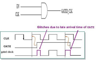
The latch-free clock gating style uses a simple AND or OR gate (depending on the edge on which flip-flops are triggered). Here if enable signal goes inactive in between the clock pulse or if it multiple times then gated clock output either can terminate prematurely or generate multiple clock pulses. This restriction makes the latch-free clock gating style inappropriate for our single-clock flip-flop based design

Latch free clock gating


Latch based clock gating

The latch-based clock gating style adds a level-sensitive latch to the design to hold the enable signal from the active edge of the clock until the inactive edge of the clock. Since the latch captures the state of the enable signal and holds it until the complete clock pulse has been generated, the enable signal need only be stable around the rising edge of the clock, just as in the traditional ungated design style.

Specific clock cells are required in library to be utilized by the synthesis tools. Availability of clock gating cells and automatic insertion by the EDA tools makes it simpler method of low power technique. Advantage of this method is that clock gating does not require modifications to RTL description.


References

[1] Frank Emnett and Mark Biegel, “Power Reduction Through RTL Clock Gating”, SNUG, San Jose, 2000

[2] PrimeTime User Guide

STA vs Gate-level Simulation

Hi all,

This post tries to explains the basic differences between Static Timing Analysis ( STA ) and Gate-Level Simulations ( Dynamic Timing Analysis )

Dynamic Timing Analysis :

  1. The design is simulated in full timing mode.
  2. Not all possibilities tested as it is dependent on the input test vectors.
  3. Simulations in full timing mode are slow and require a lot of memory.
  4. Best method to check asynchronous interfaces or interfaces between different timing domains.
  5. Requires huge amount of computing resources (CPU time, disk space for the waveforms, etc.).
  6. Helps to validate the constraints mentioned during synthesis like false paths, multi-cycle paths, etc.
  7. Helps validate your formal verification like set_comparison and set_equivalent constraints etc
  8. Reset sequences are also more problematic in gate-level simulations, so this is a common place to catch them. Synchronous reset issues that cause unknowns to pass into the flops when the reset is synthesized as part of the logic can be caught explicitly in gate-level simulation.
  9. Validation of cross-clock domain false/multicycle paths, user defined modes of operation with case_analysis and clock phase relationships can be error-prone.
  10. Helps to validate the most critical power up sequences in the design

Static timing Analysis :

  1. The delays over all paths are added up.
  2. All possibilities, including false paths, verified without the need for test vectors.
  3. Much faster than simulations, hours as opposed to days.
  4. Not good with asynchronous interfaces or interfaces between different timing domains.

Static verification methodologies such as static timing analysis and formal verification are required to meet aggressive schedules, since they reduce the need to run full back annotated regression. However, it must be understood that the static verification environments are constraint based. Therefore, the analysis is only as accurate as the constraints that drive it.


With respect to static vs. dynamic timing verification, I think it is of primary importance that all asynchronous interfaces are thoroughly stressed in back annotated simulations. In most multi-clock domain designs, many or all of the clocks are treated as false paths in static timing analysis. I think back annotated simulations are the most dependable method of verifying the correct implementation of synchronizers and FIFO's at asynchronous boundaries, and consider back annotated simulations a necessary sign-off step before tapeout.

Minimum Depth of FIFO required

Hi all,

Consider a case in which there are two systems SystemA & SystemB working with two different clocks clkA (100MHz)& clkB (70MHz) correspondingly. Both these clocks are asynchronous to each other . Data has to be communicated from SystemA to SystemB. SystemA is capable writing 70 words of data in 100 clock cycles, while SystemB is capable of reading data in each and every clock cycle.


Design a FIFO with minimum depth for the above specifications

Clock generation using Blocking or Non blocking statements

Hi all,

Consider the following two blocks of code


initial #1 clk1 = 0 ;
always @ ( clk1 )
#10 clk1 = ~clk1 ;

initial #1 clk2 = 0 ;
always @ ( clk2 )
#10 clk2 <= ~clk2 ;


What is the difference between the following two block of statements

Blocking vs Non blocking statements

Hi all,

Check the code below


module test;
reg clk,clk1,q,q1,d;

initial
begin
clk = 1'b0;
clk1 = 1'b0;
d = 1'b0;

#15 d <= 1'b1;
end

always
#5 clk = ~clk;
always
#5 clk1 <= ~clk1;

always @(posedge clk)
begin
q<=d;
end

always @(posedge clk1)
begin
q1<=d;
end

initial
begin
$monitor($realtime,"\t clk = %b, clk1 = %b, q = %b, q1 = %b, d = %b ",clk,clk1,q,q1,d);
#100 $finish;
end
endmodule


What is the output of the code above, justify it

Question on File Handling

Hi all, This is a question on file handling


integer FH ;

initial
FH = $fopen("filename1","r");


Consider the code mentioned above, What would be the value of FH if the the
file "filename1" does not exist ? Would this result in a simulation error ? Justify ?

Difference between conditional operator & if .. else

Hi all,

Consider the following verilog code

module if_cond ;
reg [1:0] a,b ;
reg [1:0] c2 ;
wire [1:0] c1 ;
reg [1:0] foo ;

assign c1 = foo ? a : b ;

always @ ( foo or a or b )
begin
if ( foo )
c2 = a ;
else
c2 = b ;
end

endmodule

What is the difference between the variables C1 & C2 ? Is there any ?

Saturday, August 2, 2008

Learn to display color messages using Verilog

Hi all,

How many among you know that you can actually display color messages using Verilog ?

Using the following piece of code, one can actually display color messages ( possible on for Linux & Unix terminals )

module colour();

initial
begin
$write("%c[1;34m",27);
$display("*********** This is in blue ***********");
$write("%c[0m",27);

$display("%c[1;31m",27);
$display("*********** This is in red ***********");
$display("%c[0m",27);

$display("%c[4;33m",27);
$display("*********** This is in brown ***********");
$display("%c[0m",27);

$display("%c[5;34m",27);
$display("*********** This is in green ***********");
$display("%c[0m",27);

$display("%c[7;34m",27);
$display("*********** This is in Back groung colour ***********");
$display("%c[0m",27);


end
endmodule


Code developed by Gopi

Tuesday, July 29, 2008

How many times does the "for" loop gets executed

Hi all,

How many times does the for loop gets executed in the following verilog code

reg [3:0] loop ;

for ( loop = 0 ; loop <= 15 ; loop = loop + 1 )
begin
$display("Inside the loop for the %d time",loop);
end

Design a XOR gate using the following custom gates


This particular one was given in an interview at IBM over 10 years ago.

Due to the war in the land of Logicia there is a shortage of XOR gates. Unfortunately, the only logic gates available are two weird components called “X” and “Y”. The truth table of both components is presented below - Z represents a High-Z value on the output.
Could you help the poor engineers of Logicia to build an XOR gate?

Model a buffer of 20 units in verilog

HI all, Which is the correct way of modeling a buffer of 20 units in verilog

Option 1 : #20 a = b ;
Option 2 : a = #20 b ;
Option 3 : #20 a <= b ;
Option 4 : a <= #20 b ;

Difference between these two verilog statements

Hi all, Can you find the difference between these two verilog (VERILOG-1995) statements


$fopen("filename");
$fopen("filename","w");


There is more than one difference ....

Monday, July 28, 2008

Interview Questions

* Define setup window and hold window ?
* What is the effect of clock skew on setup and hold ?
* In a multicycle path, where do we analyze setup and where do we analyze hold ?
* How many test clock domains are there in a chip ?
* How enables of clock gating cells are taken care at the time of scan ?
* Difference between functional coverage and code coverage ?
* Does 100% code coverage means 100% functional coverage & vice versa?
* What do you mean by useful skew ?
* What is shift miss and capture miss in transition delay faults ?
* What is the structure of clock gating cell ?
* How can you say that placing clock gating cells at synthesis level will reduce the area of the design ?
* How will you decide to insert the clock gating cell on logic where data enable is going for n number of flops
* What is the concept of synchronizers ?
* What are lockup latches?
* What is the concept of power islands ?
* What does OCV, Derate and CRPR mean in STA ?
* What is dynamic power estimation ?
* On AHB bus which path would you consider for worst timing ?
* What is the difference between blocking & non-blocking statements in verilog ?
* What are the timing equations for setup and hold, with & without considering timing skew ?
* Design a XOR gate with 2-input NAND gates
* Design AND gate with 2X1 MUX
* Design OR gate with 2X1 MUX
* Design T-Flip Flop using D-Flip Flop
* In a synchronizer how you can ensure that the second stage flop is getting stabilized input?
* Design a pulse synchronizer
* Calculate the depth of a buffer whose clock ratio is 4:1 (wr clock is fatser than read clock)
* Design a circuit that detects the negedge of a signal. The output of this circuit should get deasserted along with the input signal
* Design a DECODER using DEMUX
* Design a FSM for 10110 pattern recognition
* 80 writes in 100 clock cycles, 8 reads in 10 clock cycles. What is the minimum depth of FIFO?
* Why APB instead of AHB ?
* case, casex, casez if synthesized what would be the hardware
* Define monitor functions for AHB protocol checker
* What is the use of AHB split, give any application
* Can we synchronize data signals instead of control signals ?